Intel is confident that its angstrom-level 18A manufacturing process will surpass TSMC’s 2nm N2 technology and enter mass production much earlier.
Intel is on track with its plan to master five advanced manufacturing processes over four years and is now ready to introduce its angstrom-level 20A (2nm) and 18A (1.8nm) technologies ahead of competitors like TSMC and Samsung. Intel’s CEO, Pat Gelsinger, believes that the Intel 18A, which is scheduled for mass product use in the second half of 2024, is “slightly ahead” of TSMC’s N2 (2nm) technology planned for the second half of 2025.
The 20A and 18A processes from Intel have brought two major innovations: gate-all-around (GAA) field-effect transistors and PowerVia, a technology for power delivery to the semiconductor crystal from its backside. Intel 20A is expected to explore all the features of these innovations, while Intel 18A aims to be a “technological springboard” for Intel to reclaim its leadership in the semiconductor industry. Intel plans to start implementing the 18A process in its factories in the first quarter of 2024, with the first products based on it becoming available in the second half of 2024.
TSMC plans to begin mass production of its 2nm N2 process only in the second half of 2025. Although TSMC’s N2 will utilize GAA transistors, unlike Intel, it will retain a traditional power delivery scheme. Despite this, TSMC claims that its improved N3P technology, set to appear in 2024, will offer power, performance, and transistor density comparable to Intel’s 18A, and N2 will surpass both N3P and Intel 18A.
Gelsinger disagrees, asserting that Intel’s 18A will significantly outperform TSMC’s N2 in terms of performance and energy efficiency. He also suggested that the implementation of N2 might eventually prove to be more costly for TSMC, giving Intel’s processes a considerable competitive advantage.
Intel’s confidence in its 18A process underscores the increasingly competitive landscape of semiconductor manufacturing. Intel’s focus on innovative technologies like PowerVia and GAA transistors not only aims to enhance the performance and efficiency of its chips but also signals a strategic shift to regain market leadership. This competition drives technological advancements that are crucial for the future of computing, including the development of more powerful, energy-efficient processors suitable for a wide range of applications, from consumer electronics to high-performance computing systems. The success of Intel’s 18A process could have far-reaching implications, potentially influencing market dynamics and setting new standards in semiconductor technology.
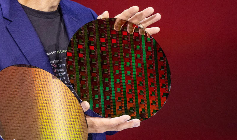
Intel’s 18A manufacturing process represents a significant advancement in semiconductor technology, set to begin manufacturing in the latter half of 2024. Here are the key aspects of Intel’s 18A technology:
- Introduction of Breakthrough Technologies: Intel 18A incorporates two major breakthroughs: PowerVia and RibbonFET. PowerVia is an innovative approach to power delivery, optimizing the way power is supplied to the chip. RibbonFET, Intel’s first new transistor architecture since FinFET, represents a gate-all-around (GAA) transistor design, which is expected to improve performance and power efficiency significantly.
- Refinement of Existing Technologies: The 18A process will refine the RibbonFET and PowerVia technologies, focusing on shrinking transistor sizes further. This refinement indicates a continued push towards increasing the density of transistors on a chip, which is a key factor in enhancing overall chip performance and efficiency.
- Manufacturing Timeline and Applications: Intel is set to begin manufacturing using the 18A process in the latter half of 2024. It is anticipated that this advanced node will be used to produce future consumer Lake CPUs, marking a significant step in Intel’s roadmap towards more advanced and efficient processors.
- Future Expectations: The 18A process is a part of Intel’s roadmap leading up to 2025. This timeline suggests that Intel is positioning the 18A process as a cornerstone of its future semiconductor technology, potentially influencing a wide range of future products and applications. For instance, the Panther Lake client platform, expected around 2025, will utilize the technological advancements of the 18A node, following the Lunar Lake processors set for a 2024-2025 timeframe.
The development of the Intel 18A process node is indicative of Intel’s commitment to innovation in the semiconductor industry. By introducing groundbreaking technologies like PowerVia and RibbonFET, Intel aims to enhance the performance, efficiency, and capabilities of its future processors. This development is crucial in the context of the ever-increasing demand for more powerful and energy-efficient computing solutions in various sectors, ranging from consumer electronics to complex enterprise systems.